ST STM32H7B3I Discovery Kit
Overview
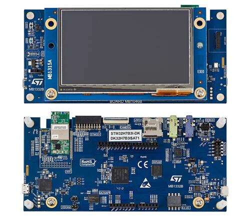
The STM32H7B3I-DK Discovery kit is a complete demonstration and development platform for STMicroelectronics Arm® Cortex®-M7 core-based STM32H7B3LIH6QU microcontroller.
The STM32H7B3I-DK Discovery kit is used as a reference design for user application development before porting to the final product, thus simplifying the application development.
The full range of hardware features available on the board helps users enhance their application development by an evaluation of almost all peripherals (such as USB OTG_HS, microSD, USART, FDCAN, audio DAC stereo with audio jack input and output, camera, SDRAM, Octo-SPI Flash memory and RGB interface LCD with capacitive touch panel). ARDUINO® Uno V3 connectors provide easy connection to extension shields or daughterboards for specific applications.
STLINK-V3E is integrated into the board, as an embedded in-circuit debugger and programmer for the STM32 MCU and the USB Virtual COM port bridge. The STM32H7B3I-DK board comes with the STM32CubeH7 MCU Package, which provides an STM32 comprehensive software HAL library as well as various software examples.
More information about the board can be found at the STM32H7B3I-DK website. More information about STM32H7B3 can be found here:
Supported Features
The current Zephyr stm32h7b3i_dk board configuration supports the following hardware features:
Interface |
Controller |
Driver/Component |
|---|---|---|
NVIC |
on-chip |
nested vector interrupt controller |
UART |
on-chip |
serial port-polling; serial port-interrupt |
PINMUX |
on-chip |
pinmux |
GPIO |
on-chip |
gpio |
I2C |
on-chip |
i2c |
FLASH |
on-chip |
flash memory |
FMC |
on-chip |
memc (SDRAM) |
LTDC |
on-chip |
display |
CANFD |
on-chip |
can |
Other hardware features have not been enabled yet for this board.
The default configuration per core can be found in the defconfig file:
boards/arm/stm32h7b3i_dk/stm32h7b3i_dk_defconfig
Pin Mapping
For more details please refer to STM32H7B3I-DK website.
Default Zephyr Peripheral Mapping:
UART_1 TX/RX : PA9/PA10 (ST-Link Virtual Port Com)
UART_4 TX/RX : PH13/PH14 (Arduino Serial)
I2C4 SCL/SDA : PD12/PD13 (Arduino I2C, Touchscreen FT5336 with PH2 Interrupt Pin)
SPI2 SCK/MISO/MOSI/NSS : PA12/PB14/PB15/PI0 (Arduino SPI)
LD1 : PG11
LD2 : PG2
USER_PB : PC13
SDMMC D0/D1/D2/D3/CK/CMD/CD : PC8/PC9/PC10/PC11/PC12/PD2/PI8
CANFD RX/TX/WAKE [1] : PA11/PA12/PH8
FMC SDRAM :
D0-D15 : PD14/PD15/PD0/PD1/PE7/PE8/PE9/PE10/PE11/PE12/PE13/PE14/PE15/PD8/PD9/PD10
A0-A11 : PF0/PF1/PF2/PF3/PF4/PF5/PF12/PF13/PF14/PF15/PG0/PG1
A14/A15 : PG4/PG5
SDNRAS/SDNCAS : PF11/PG15
NBL0/NBL1 : PE0/PE1
SDCLK/SDNWE/SDCKE1/SDNE1 : PG8/PH5/PH7/PH6
LTDC :
R0-R7 : PI15/PJ0/PJ1/PJ2/PJ3/PJ4/PJ5/PJ6
G0-G7 : PJ7/PJ8/PJ9/PJ10/PJ11/PK0/PK1/PK2
B0-B7 : PJ12/PK13/PJ14/PJ15/PK3/PK4/PK5/PK6
DE/CLK/HSYNC/VSYNC : PK7/PI14/PI12/PI13
System Clock
The STM32H7B3I System Clock can be driven by an internal or external oscillator, as well as by the main PLL clock. By default, the System clock is driven by the PLL clock at 280MHz. PLL clock is fed by a 24MHz high speed external clock.
Serial Port
The STM32H7B3I Discovery kit has up to 8 UARTs. The Zephyr console output is assigned to UART1 which connected to the onboard ST-LINK/V3.0. Virtual COM port interface. Default communication settings are 115200 8N1.
Programming and Debugging
See Building an Application for more information about application builds.
Flashing
Flashing operation will depend on the target to be flashed and the SoC
option bytes configuration.
It is advised to use STM32CubeProgrammer to check and update option bytes
configuration and flash the stm32h7b3i_dk target.
Debugging
You can debug an application in the usual way. Here is an example for the Hello World application.
# From the root of the zephyr repository
west build -b stm32h7b3i_dk samples/hello_world
west debug