Redbear Labs Nano v2
Overview
The Nano v2 is a development board equipped with Nordic’s next generation nRF52832 Bluetooth Low Energy SOC. This board was designed as a ‘drop-in’ replacement of BLE Nano with exactly the same form factor.
Hardware
nRF52832 SoC is built around a 32-bit ARM Cortex-M4F CPU with 512kB flash + 64kB RAM
11 x Digital I/0
1 UART with hardware flow control ( 4 I/O pins occupied )
1 I2C ( 2 I/O pins occupied )
Supported Features
The BLE Nano v2 board configuration supports the following hardware features:
Interface |
Controller |
Driver/Component |
|---|---|---|
NVIC |
on-chip |
nested vectored interrupt controller |
UART |
on-chip |
serial port |
GPIO |
on-chip |
gpio |
FLASH |
on-chip |
flash |
RADIO |
on-chip |
Bluetooth |
I2C |
on-chip |
i2c |
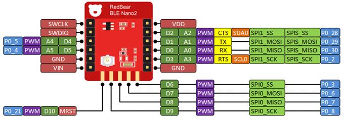
Connections and IOs
BLE nano v2 pinout
DAPLink board
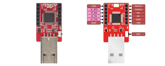
The DAPLink USB board acts as a dongle. DAPLink debug probes appear on the host computer as a USB disk. It also regulates 5V from USB to 3.3V via the onboard LDO to power Nano v2.
Programming and Debugging
Applications for the nrf52_blenano2 board configuration can be built and
flashed in the usual way (see Building an Application and
Run an Application for more details).
Flashing
To flash an application, you’ll need to connect your BLE Nano 2 with the DAPLink board, then attach that to your computer via USB.
Warning
Be careful to mount the BLE Nano 2 correctly! The side of the board with the VIN and GND pins should face towards the USB connector.
Now build and flash applications as usual. Here is an example for the Hello World application.
# From the root of the zephyr repository
west build -b nrf52_blenano2 samples/hello_world
west flash
Debugging
After mounting the BLE Nano 2 on its DAPLink board as described above, you can debug an application in the usual way. Here is an example for the Hello World application.
# From the root of the zephyr repository
west build -b nrf52_blenano2 samples/hello_world
west debug