STM32 Mini F401
Overview
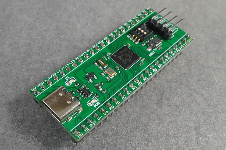
The STM32 Mini F401 is an extremely low cost and bare-bones development board featuring the STM32F401CC, see STM32F401CC website [4]. More info about the board with schematics available here [2]
Hardware
The STM32F401CC based board provides the following hardware components:
STM32F401CCU6 in UFQFPN48 package
ARM® 32-bit Cortex® -M4 CPU with FPU
84 MHz max CPU frequency
VDD from 1.7 V to 3.6 V
256 KB Flash
64 KB SRAM
GPIO with external interrupt capability
1x12-bit, 2.4 MSPS ADC with 16 channels
DMA Controller
Up to 11 Timers (six 16-bit, two 32-bit, two watchdog timers and a SysTick timer)
USART/UART (3)
I2C (3)
SPI/I2S (4)
SDIO
USB 2.0 full-speed device/host/OTG controller with on-chip PHY
CRC calculation unit
96-bit unique ID
RTC
Supported Features
The Zephyr stm32f401_mini board configuration supports the following hardware features:
Interface |
Controller |
Driver/Component |
|---|---|---|
NVIC |
on-chip |
nested vector interrupt controller |
SYSTICK |
on-chip |
system clock |
UART |
on-chip |
serial port |
GPIO |
on-chip |
gpio |
PINMUX |
on-chip |
pinmux |
FLASH |
on-chip |
flash |
SPI |
on-chip |
spi |
I2C |
on-chip |
i2c |
ADC |
on-chip |
ADC Controller |
USB OTG FS |
on-chip |
USB device |
The default configuration can be found in the defconfig file:
boards/arm/stm32f401_mini/stm32f401_mini_defconfig
Default Zephyr Peripheral Mapping:
UART_1 TX/RX : PA9/PA10
I2C1 SCL/SDA : PB8/PB9
SPI1 CS/SCK/MISO/MOSI : PA4/PA5/PA6/PA7
PWM_4_CH1 : PB6
PWM_4_CH2 : PB7
ADC_1 : PA1
SW0 : PB2 (routed to BOOT1 dip switch)
LED0 : PC13
Clock Sources
The board has two external oscillators. The frequency of the slow clock (LSE) is 32.768 kHz. The frequency of the main clock (HSE) is 25 MHz.
The default configuration sources the system clock from the PLL, which is derived from HSE, and is set at 84MHz.
Programming and Debugging
There are 2 main entry points for flashing STM32F4X SoCs, one using the ROM bootloader, and another by using the SWD debug port (which requires additional hardware). Flashing using the ROM bootloader requires a special activation pattern, which can be triggered by using the BOOT0 pin, which on this board is a dip switch.
Flashing
Installing dfu-util
It is recommended to use at least v0.8 of dfu-util [3]. The package available in debian/ubuntu can be quite old, so you might have to build dfu-util from source.
There is also a Windows version which works, but you may have to install the right USB drivers with a tool like Zadig [1].
Flashing an Application
Connect a USB-C cable and the board should power ON. Force the board into DFU mode by setting the BOOT0 dip switch position to ON. Reset the board with the NRST button.
The dfu-util runner is supported on this board and so a sample can be built and tested easily.
# From the root of the zephyr repository
west build -b stm32f401_mini samples/basic/blinky
west flash
Debugging
The board can be debugged by installing the included 100 mil (0.1 inch) header, and attaching an SWD debugger to the 3V3 (3.3V), GND, SCK, and DIO pins on that header.