Raytac MDBT53V-DB-40
Overview
Raytac MDBT53V-DB-40 demo board is a development board based on the Raytac MDBT53V-1M module, using Nordic Semiconductor nRF5340 ARM Cortex-M33 SoC. Its design concept is to connect all of the module’s pins to 2.54mm pin headers. It is convenient for developers to verify whether the modules are connected to other peripheral devices or sensors as a tool for software development.
The nRF5340 inside the MDBT53V-1M module is a dual-core SoC based on the Arm® Cortex®-M33 architecture, with:
a full-featured Arm Cortex-M33F core with DSP instructions, FPU, and Armv8-M Security Extension, running at up to 128 MHz, referred to as the application core
a secondary Arm Cortex-M33 core, with a reduced feature set, running at a fixed 64 MHz, referred to as the network core.
The raytac_mdbt53v_db_40_nrf5340_cpuapp build target provides support for the application core on the nRF5340 SoC. The raytac_mdbt53v_db_40_nrf5340_cpuapp build target provides support for the network core on the nRF5340 SoC.
nRF5340 SoC provides support for the following devices:
ADC
CLOCK
FLASH
GPIO
IDAU
I2C
MPU
NVIC
PWM
RADIO (Bluetooth Low Energy and 802.15.4)
RTC
Segger RTT (RTT Console)
SPI
UARTE
WDT
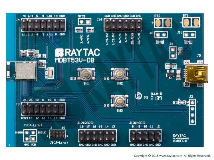
MDBT53V-DB-40 (Credit: Raytac Corporation)
More information about the board can be found at the MDBT53V-DB-40 website. The MDBT53V-DB-40 Specification contains the demo board’s datasheet. The MDBT53V-DB-40 Schematic contains the demo board’s schematic.
Hardware
Module Demo Board build by MDBT53V-1M
Nordic nRF5340 SoC Solution
A recommnded 3rd-party module by Nordic Semiconductor.
Dual-core Arm® Cortex® M33
1MB/256KB Flash Memory; 512kB/ 64kB RAM
Supports BT5 Long Range Features
Bluetooth specification v5.2
Supports BT5 Long Range Features
Supports Bluetooth Direction Finding & Mesh
Supports Bluetooth low energy audio
Cerifications: FCC, IC, CE, Telec(MIC), KC, SRRC, NCC, RCM, WPC
RoHs & Reach Compiant.
25 GPIO
Chip Antenna
Interfaces: SPI, UART, I2C, I2S, PWM, ADC, and NFC
Highly flexible multiprotocol SoC ideally suited for Bluetooth® Low Energy, ANT+, Zigbee, Thread (802.15.4) ultra low-power wireless applications.
1 User LEDs
3 User buttons
1 Mini USB connector for power supply
SWD connector for FW programing
J-Link interface for FW programing
Supported Features
The raytac_mdbt53v_db_40_nrf5340_cpuapp board configuration supports the following hardware features:
Interface |
Controller |
Driver/Component |
|---|---|---|
ADC |
on-chip |
adc |
CLOCK |
on-chip |
clock_control |
FLASH |
on-chip |
flash |
GPIO |
on-chip |
gpio |
I2C(M) |
on-chip |
i2c |
MPU |
on-chip |
arch/arm |
NVIC |
on-chip |
arch/arm |
PWM |
on-chip |
pwm |
RTC |
on-chip |
system clock |
SPI(M/S) |
on-chip |
spi |
UARTE |
on-chip |
serial |
WDT |
on-chip |
watchdog |
The raytac_mdbt53v_db_40_nrf5340_cpunet board configuration supports the following hardware features:
Interface |
Controller |
Driver/Component |
|---|---|---|
CLOCK |
on-chip |
clock_control |
FLASH |
on-chip |
flash |
GPIO |
on-chip |
gpio |
I2C(M) |
on-chip |
i2c |
MPU |
on-chip |
arch/arm |
NVIC |
on-chip |
arch/arm |
RADIO |
on-chip |
Bluetooth, ieee802154 |
RTC |
on-chip |
system clock |
SPI(M/S) |
on-chip |
spi |
UARTE |
on-chip |
serial |
WDT |
on-chip |
watchdog |
Other hardware features have not been enabled yet for this board. See MDBT53V-DB-40 website and MDBT53V-DB-40 Specification for a complete list of Raytac MDBT53V-DB-40 board hardware features.
Connections and IOs
LED
LED1 (green) = P0.31
HSPI
MOSI = P0.9
MISO = P0.10
SCK = P0.8
CSN = P0.11
DCX = P0.12
QSPI
SCK = P0.17
CSN = P0.18
DATA0 = P0.13
DATA1 = P0.14
DATA2 = P0.15
DATA3 = P0.16
Security components
Implementation Defined Attribution Unit (IDAU) on the application core. The IDAU is implemented with the System Protection Unit and is used to define secure and non-secure memory maps. By default, all of the memory space (Flash, SRAM, and peripheral address space) is defined to be secure accessible only.
Secure boot.
Programming and Debugging
nRF5340 application core supports the Armv8-M Security Extension. Applications built for the raytac_mdbt53v_db_40_nrf5340_cpuapp board by default boot in the Secure state.
nRF5340 network core does not support the Armv8-M Security Extension. nRF5340 IDAU may configure bus accesses by the nRF5340 network core to have Secure attribute set; the latter allows to build and run Secure only applications on the nRF5340 SoC.
Applications for the raytac_mdbt53v_db_40_nrf5340 board configuration can be
built, flashed, and debugged in the usual way. See Building an Application and
Run an Application for more details on building and running.
Note
Flashing and Debugging Zephyr onto the raytac_mdbt53v_db_40_nrf5340 board requires an external J-Link programmer. The programmer is attached to the J1 or J9 SWD connector.
Flashing
Follow the instructions in the Nordic nRF5x Segger J-Link page to install and configure all the necessary software. Further information can be found in Flashing. Then build and flash applications as usual (see Building an Application and Run an Application for more details).
Here is an example for the Hello World application.
Use a USB to TTL converter to connect the computer and raytac_mdbt53v_db_40_nrf5340 J13 connector pin 8(RX), 9(TX) and GND. Then run your favorite terminal program to listen for output.
$ minicom -D <tty_device> -b 115200
Replace <tty_device> with the port where the USB to TTL converter
can be found. For example, under Linux, /dev/ttyUSB0.
Then build and flash the application in the usual way.
# From the root of the zephyr repository
west build -b raytac_mdbt53v_db_40_nrf5340 samples/hello_world
west flash
Debugging
The raytac_mdbt53v_db_40_nrf5340 board does not have an on-board-J-Link debug IC,
however, instructions from the Nordic nRF5x Segger J-Link page also apply to this board.
Use the Debug out connector of nRF52x DK to connect to the J1 connector, and use SEGGER
J-Link OB IF to debug.