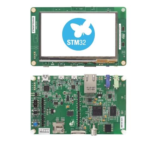
ST STM32F7508-DK Discovery Kit
Overview
The discovery kit enables a wide diversity of applications taking benefit from audio, multi-sensor support, graphics, security, security, video, and high-speed connectivity features. Important board features include:
STM32F750N8H6 microcontroller featuring 64 Kbytes of Flash memory and 340 Kbytes of RAM, in BGA216 package
On-board ST-LINK/V2-1 supporting USB re-enumeration capability
Five power supply options:
ST LINK/V2-1
USB FS connector
USB HS connector
VIN from Arduino connector
External 5 V from connector
Two pushbuttons (user and reset)
USB functions: virtual COM port, mass storage, debug port
4.3-inch 480x272 color LCD-TFT with capacitive touch screen
SAI audio codec
Audio line in and line out jack
Two ST MEMS microphones
SPDIF RCA input connector
128-Mbit Quad-SPI Flash memory
128-Mbit SDRAM (64 Mbits accessible)
Connector for microSD card
USB OTG HS with Micro-AB connectors
USB OTG FS with Micro-AB connectors
Ethernet connector compliant with IEEE-802.3-2002
More information about the board can be found at the 32F7508-DK website.
Hardware
The STM32F7508-DK Discovery kit provides the following hardware components:
STM32F750N8H6 in BGA216 package
ARM® 32-bit Cortex® -M7 CPU with FPU
216 MHz max CPU frequency
64 KB Flash
320+16+4 KB SRAM
GPIO with external interrupt capability
4.3-inch 480x272 color LCD-TFT with capacitive touch screen
3x12-bit ADC
2x12-bit D/A converters
RTC
Advanced-control Timer
General Purpose Timers (17)
Watchdog Timers (2)
USART/UART (8)
I2C (4)
SPI (6)
2xSAI (serial audio interface)
2xCAN
USB 2.0 OTG FS with on-chip PHY
USB 2.0 OTG HS/FS with dedicated DMA, on-chip full-speed PHY and ULPI
10/100 Ethernet MAC with dedicated DMA
8- to 14-bit parallel camera
CRC calculation unit
True random number generator
DMA Controller
More information about STM32F750x8 can be found here:
Supported Features
The Zephyr stm32f7508_dk board configuration supports the following hardware features:
Interface |
Controller |
Driver/Component |
|---|---|---|
NVIC |
on-chip |
nested vector interrupt controller |
UART |
on-chip |
serial port-polling; serial port-interrupt |
PINMUX |
on-chip |
pinmux |
GPIO |
on-chip |
gpio |
FLASH |
on-chip |
flash memory |
ETHERNET |
on-chip |
Ethernet |
PWM |
on-chip |
pwm |
I2C |
on-chip |
i2c |
USB |
on-chip |
usb |
SDMMC |
on-chip |
disk access |
SPI |
on-chip |
spi |
QSPI NOR |
on-chip |
off-chip flash |
FMC |
on-chip |
memc (SDRAM) |
LTDC |
on-chip |
display |
Other hardware features are not yet supported on Zephyr porting.
The default configuration can be found in the defconfig file:
boards/arm/stm32f7508_dk/stm32f7508_dk_defconfig
Pin Mapping
STM32F7508-DK Discovery kit has 9 GPIO controllers. These controllers are responsible for pin muxing, input/output, pull-up, etc.
For more details please refer to 32F7508-DK board User Manual.
Default Zephyr Peripheral Mapping:
The STM32F7508 Discovery kit features an Arduino Uno V3 connector. Board is configured as follows
UART_1 TX/RX : PA9/PB7 (ST-Link Virtual Port Com)
UART_6 TX/RX : PC6/PC7 (Arduino Serial)
I2C1 SCL/SDA : PB8/PB9 (Arduino I2C)
SDMMC_1 D0/D1/D2/D3/CK/CD/CMD: PC8/PC9/PC10/PC11/PC12/PC13/PD2
SPI2 NSS/SCK/MISO/MOSI : PA8/PI1/PB14/PB15 (Arduino SPI)
PWM_3_CH1 : PB4
ETH : PA1, PA2, PA7, PC1, PC4, PC5, PG11, PG13, PG14
USER_PB : PI11
LD1 : PI1
USB DM : PA11
USB DP : PA12
FMC SDRAM :
D0-D15 : PD14/PD15/PD0/PD1/PE7/PE8/PE9/PE10/PE11/PE12/PE13/PE14/PE15/PD8/PD9/PD10
A0-A11 : PF0/PF1/PF2/PF3/PF4/PF5/PF12/PF13/PF14/PF15/PG0/PG1
A14/A15 : PG4/PG5
SDNRAS/SDNCAS : PF11/PG15
NBL0/NBL1 : PE0/PE1
SDCLK/SDNWE/SDCKE0/SDNE0 : PG8/PH5/PC3/PH3
LTDC :
R0-R7 : PI15/PJ0/PJ1/PJ2/PJ3/PJ4/PJ5/PJ6
G0-G7 : PJ7/PJ8/PJ9/PJ10/PJ11/PK0/PK1/PK2
B0-B7 : PJ12/PK13/PJ14/PJ15/PK3/PK4/PK5/PK6
DE/CLK/HSYNC/VSYNC : PK7/PI14/PI12/PI13
System Clock
The STM32F7508 System Clock can be driven by an internal or external oscillator, as well as by the main PLL clock. By default, the System clock is driven by the PLL clock at 216MHz, driven by a 25MHz high speed external clock.
Serial Port
The STM32F7508-DK Discovery kit has up to 8 UARTs. The Zephyr console output is assigned to UART1 which connected to the onboard ST-LINK/V2 Virtual COM port interface. Default communication settings are 115200 8N1.
Programming and Debugging
Applications for the stm32f7508_dk board configuration can be built and
flashed in the usual way (see Building an Application and
Run an Application for more details).
Flashing
STM32F7508-DK Discovery kit includes an ST-LINK/V2 embedded debug tool interface. This interface is supported by the openocd version included in the Zephyr SDK.
Flashing an application to STM32F7508-DK
First, connect the STM32F746G Discovery kit to your host computer using the USB port to prepare it for flashing. Then build and flash your application.
Here is an example for the Hello World application.
# From the root of the zephyr repository
west build -b stm32f7508_dk samples/hello_world
west flash
Run a serial host program to connect with your board:
$ minicom -D /dev/ttyACM0
You should see the following message on the console:
Hello World! arm
Debugging
You can debug an application in the usual way. Here is an example for the Hello World application.
# From the root of the zephyr repository
west build -b stm32f7508_dk samples/hello_world
west debug