Laird Connectivity BL653 DVK
Overview
The BL653 Development Kit (453-00039-K1, 453-00041-K1) hardware provides support for the Laird Connectivity BL653 module powered by a Nordic Semiconductor nRF52833 ARM Cortex-M4F CPU.
This development kit has the following features:
ADC
CLOCK
FLASH
GPIO
I2C
MPU
NVIC
PWM
RADIO (Bluetooth Low Energy and 802.15.4)
RTC
Segger RTT (RTT Console)
SPI
UART
USB
WDT
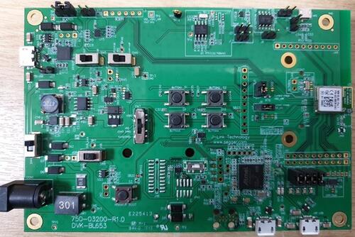
BL653 Development Kit Board
More information about the board can be found at the BL653 website [1].
Hardware
Supported Features
The BL653 DVK board configuration supports the following hardware features:
Interface |
Controller |
Driver/Component |
|---|---|---|
ADC |
on-chip |
adc |
CLOCK |
on-chip |
clock_control |
FLASH |
on-chip |
flash |
GPIO |
on-chip |
gpio |
I2C(M) |
on-chip |
i2c |
MPU |
on-chip |
arch/arm |
NVIC |
on-chip |
arch/arm |
PWM |
on-chip |
pwm |
RADIO |
on-chip |
Bluetooth, ieee802154 |
RTC |
on-chip |
system clock |
RTT |
Segger |
console |
SPI(M/S) |
on-chip |
spi |
UART |
on-chip |
serial |
USB |
on-chip |
usb |
WDT |
on-chip |
watchdog |
Other hardware features have not been enabled yet for this board. See BL653 website [1] for a complete list of BL653 Development Kit board hardware features.
Connections and IOs
LED
LED1 (blue) = P0.13
LED2 (blue) = P0.14
LED3 (blue) = P0.15
LED4 (blue) = P0.16
Programming and Debugging
Applications for the bl653_dvk board configuration can be built, flashed,
and debugged in the usual way. See Building an Application and
Run an Application for more details on building and running.
Flashing
Follow the instructions in the Nordic nRF5x Segger J-Link page to install and configure all the necessary software. Further information can be found in Flashing. Then build and flash applications as usual (see Building an Application and Run an Application for more details).
Here is an example for the Hello World application.
First, run your favorite terminal program to listen for output.
NOTE: On the BL653 development board, the FTDI USB should be used to access the UART console.
$ minicom -D <tty_device> -b 115200
Replace <tty_device> with the port where the BL653 development kit
can be found. For example, under Linux, /dev/ttyUSB0.
Then build and flash the application in the usual way.
# From the root of the zephyr repository
west build -b bl653_dvk samples/hello_world
west flash
Debugging
Refer to the Nordic nRF5x Segger J-Link page to learn about debugging Nordic based boards with a Segger IC.
Testing Bluetooth on the BL653 DVK
Many of the Bluetooth examples will work on the BL653 DVK. Try them out:
Using UART1
The following approach can be used when an application needs to use more than one UART for connecting peripheral devices:
Add devicetree overlay file to the main directory of your application:
&pinctrl {
   uart1_default: uart1_default {
      group1 {
         psels = <NRF_PSEL(UART_TX, 0, 14)>,
                 <NRF_PSEL(UART_RX, 0, 16)>;
      };
   };
   /* required if CONFIG_PM_DEVICE=y */
   uart1_sleep: uart1_sleep {
      group1 {
         psels = <NRF_PSEL(UART_TX, 0, 14)>,
                 <NRF_PSEL(UART_RX, 0, 16)>;
         low-power-enable;
      };
   };
};

&uart1 {
  compatible = "nordic,nrf-uarte";
  current-speed = <115200>;
  status = "okay";
  pinctrl-0 = <&uart1_default>;
  pinctrl-1 = <&uart1_sleep>;
  pinctrl-names = "default", "sleep";
};
In the overlay file above, pin P0.16 is used for RX and P0.14 is used for TX
Use the UART1 as
DEVICE_DT_GET(DT_NODELABEL(uart1))
See Set devicetree overlays for further details.
Selecting the pins
Pins can be configured in the board pinctrl file. To see the available mappings, open the nRF52833 Product Specification [2], chapter 7 ‘Hardware and Layout’. In the table 7.1.1 ‘aQFN73 ball assignments’ select the pins marked ‘General purpose I/O’. Note that pins marked as ‘low frequency I/O only’ can only be used in under-10KHz applications. They are not suitable for 115200 speed of UART.