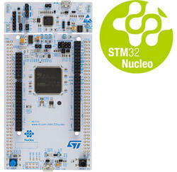
ST Nucleo L496ZG
Overview
The Nucleo L496ZG board features an ARM Cortex-M4 based STM32L496ZG MCU with a wide range of connectivity support and configurations. Here are some highlights of the Nucleo L476ZG board:
STM32 microcontroller in QFP144 package
USB OTG FS with Micro-AB connector
Two types of extension resources:
Arduino Uno V3 connectivity
ST morpho extension pin headers for full access to all STM32 I/Os
On-board ST-LINK/V2-1 debugger/programmer with SWD connector
Flexible board power supply:
USB VBUS or external source(3.3V, 5V, 7 - 12V)
Power management access point
8 LEDs: user LEDs (LD1, LD2, LD3), communication LED (LD4), USB power fault(LD5), power LED (LD6), USB FS OTG (LD7, LD8)
2 push buttons: USER and RESET
More information about the board can be found at the Nucleo L496ZG website.
Hardware
The STM32L496ZG SoC provides the following hardware capabilities:
Ultra-low-power with FlexPowerControl (down to 108 nA Standby mode and 91 uA/MHz run mode)
Core: ARM® 32-bit Cortex®-M4 CPU with FPU, frequency up to 80 MHz, 100DMIPS/1.25DMIPS/MHz (Dhrystone 2.1)
Clock Sources:
4 to 48 MHz crystal oscillator
32 kHz crystal oscillator for RTC (LSE)
Internal 16 MHz factory-trimmed RC ( ±1%)
Internal low-power 32 kHz RC ( ±5%)
Internal multispeed 100 kHz to 48 MHz oscillator, auto-trimmed by LSE (better than ±0.25 % accuracy)
3 PLLs for system clock, USB, audio, ADC
RTC with HW calendar, alarms and calibration
LCD 8 x 40 or 4 x 44 with step-up converter
Up to 24 capacitive sensing channels: support touchkey, linear and rotary touch sensors
16x timers:
2x 16-bit advanced motor-control
2x 32-bit and 5x 16-bit general purpose
2x 16-bit basic
2x low-power 16-bit timers (available in Stop mode)
2x watchdogs
SysTick timer
Up to 114 fast I/Os, most 5 V-tolerant, up to 14 I/Os with independent supply down to 1.08 V
Memories
Up to 1 MB Flash, 2 banks read-while-write, proprietary code readout protection
Up to 320 KB of SRAM including 64 KB with hardware parity check
External memory interface for static memories supporting SRAM, PSRAM, NOR and NAND memories
Quad SPI memory interface
4x digital filters for sigma delta modulator
Rich analog peripherals (independent supply)
3x 12-bit ADC 5 MSPS, up to 16-bit with hardware oversampling, 200 uA/MSPS
2x 12-bit DAC, low-power sample and hold
2x operational amplifiers with built-in PGA
2x ultra-low-power comparators
20x communication interfaces
USB OTG 2.0 full-speed, LPM and BCD
2x SAIs (serial audio interface)
4x I2C FM+(1 Mbit/s), SMBus/PMBus
5x U(S)ARTs (ISO 7816, LIN, IrDA, modem)
1x LPUART
3x SPIs (4x SPIs with the Quad SPI)
2x CAN (2.0B Active) and SDMMC interface
SWPMI single wire protocol master I/F
IRTIM (Infrared interface)
14-channel DMA controller
True random number generator
CRC calculation unit, 96-bit unique ID
Development support: serial wire debug (SWD), JTAG, Embedded Trace Macrocell™
More information about STM32L496ZG can be found here:
Supported Features
The Zephyr nucleo_l496zg board configuration supports the following hardware features:
Interface |
Controller |
Driver/Component |
|---|---|---|
NVIC |
on-chip |
nested vector interrupt controller |
UART |
on-chip |
serial port-polling; serial port-interrupt |
PINMUX |
on-chip |
pinmux |
GPIO |
on-chip |
gpio |
I2C |
on-chip |
i2c |
SPI |
on-chip |
spi |
PWM |
on-chip |
pwm |
RTC |
on-chip |
rtc |
WATCHDOG |
on-chip |
System Window Watchdog |
Other hardware features are not yet supported on this Zephyr port.
The default configuration can be found in the defconfig file:
boards/arm/nucleo_l496zg/nucleo_l496zg_defconfig
Connections and IOs
Nucleo L496ZG Board has 8 GPIO controllers. These controllers are responsible for pin muxing, input/output, pull-up, etc.
For more details please refer to STM32 Nucleo-144 board User Manual.
Default Zephyr Peripheral Mapping:
UART_2 TX/RX : PD5/PD6
UART_3 TX/RX : PD8/PD9
LPUART_1 TX/RX : PG7/PG8
PWM_1_CH1: PE9
PWM_1_CH2: PE11
PWM_1_CH3: PE13
PWM_2_CH1: PA0
I2C_1_SCL: PB8
I2C_1_SDA: PB7
SPI_1_NSS: PD14
SPI_1_SCK: PA5
SPI_1_MISO: PA6
SPI_1_MOSI: PA7
USER_PB : PC13
LD1 : PC7
LD2 : PB7
LD3 : PB14
System Clock
Nucleo L496ZG System Clock could be driven by internal or external oscillator, as well as main PLL clock. By default System clock is driven by PLL clock at 80MHz, driven by 16MHz high speed internal oscillator.
Serial Port
Nucleo L496ZG board has 5 U(S)ARTs. The Zephyr console output is assigned to UART2. Default settings are 115200 8N1.
Programming and Debugging
Applications for the nucleo_l496zg board configuration can be built and
flashed in the usual way (see Building an Application and
Run an Application for more details).
Flashing
Nucleo L496ZG board includes an ST-LINK/V2-1 embedded debug tool interface. This interface is supported by the openocd version included in the Zephyr SDK since v0.9.5.
Flashing an application to Nucleo L496ZG
Connect the Nucleo L496ZG to your host computer using the USB port. Then build and flash an application. Here is an example for the Hello World application.
Run a serial host program to connect with your Nucleo board:
$ minicom -D /dev/ttyUSB0
Then build and flash the application.
# From the root of the zephyr repository
west build -b nucleo_l496zg samples/hello_world
west flash
You should see the following message on the console:
Hello World! arm
Debugging
You can debug an application in the usual way. Here is an example for the Hello World application.
# From the root of the zephyr repository
west build -b nucleo_l496zg samples/hello_world
west debug