Laird Connectivity BL5340 DVK
Overview
The BL5340 Development Kit provides support for the Laird Connectivity BL5340 module which is powered by a dual-core Nordic Semiconductor nRF5340 ARM Cortex-M33F CPU. The nRF5340 inside the BL5340 module is a dual-core SoC based on the Arm® Cortex®-M33 architecture, with:
a full-featured Arm Cortex-M33F core with DSP instructions, FPU, and Armv8-M Security Extension, running at up to 128 MHz, referred to as the application core
a secondary Arm Cortex-M33 core, with a reduced feature set, running at a fixed 64 MHz, referred to as the network core.
The bl5340_dvk_cpuapp build target provides support for the application core on the BL5340 module. The bl5340_dvk_cpunet build target provides support for the network core on the BL5340 module. If ARM TrustZone is used then the bl5340_dvk_cpuapp build target provides support for the non-secure partition of the application core on the BL5340 module.
This development kit has the following features:
ADC
CLOCK
FLASH
GPIO
IDAU
I2C
I2S
MPU
NVIC
PWM
QSPI
RADIO (Bluetooth Low Energy and 802.15.4)
RTC
Segger RTT (RTT Console)
SPI
UARTE
USB
WDT
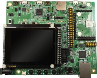
BL5340 DVK (Credit: Laird Connectivity)
More information about the module can be found on the BL5340 homepage [2].
The Nordic Semiconductor Infocenter [3] contains the processor’s information and the datasheet.
Hardware
The BL5340 DVK has two external oscillators. The frequency of the slow clock is 32.768KHz. The frequency of the main clock is 32MHz.
Supported Features
The bl5340_dvk_cpuapp board configuration supports the following hardware features:
Interface |
Controller |
Driver/Component |
|---|---|---|
ADC |
on-chip |
adc |
CLOCK |
on-chip |
clock_control |
FLASH |
on-chip |
flash |
GPIO |
on-chip |
gpio |
I2C(M) |
on-chip |
i2c |
MPU |
on-chip |
arch/arm |
NVIC |
on-chip |
arch/arm |
QSPI(M) |
on-chip |
nor |
PWM |
on-chip |
pwm |
RTC |
on-chip |
system clock |
RTT |
Segger |
console |
SPI(M/S) |
on-chip |
spi |
SPU |
on-chip |
system protection |
UARTE |
on-chip |
serial |
USB |
on-chip |
usb |
WDT |
on-chip |
watchdog |
The bl5340_dvk_cpunet board configuration supports the following hardware features:
Interface |
Controller |
Driver/Component |
|---|---|---|
CLOCK |
on-chip |
clock_control |
FLASH |
on-chip |
flash |
GPIO |
on-chip |
gpio |
I2C(M) |
on-chip |
i2c |
MPU |
on-chip |
arch/arm |
NVIC |
on-chip |
arch/arm |
RADIO |
on-chip |
Bluetooth, ieee802154 |
RTC |
on-chip |
system clock |
RTT |
Segger |
console |
SPI(M/S) |
on-chip |
spi |
UARTE |
on-chip |
serial |
WDT |
on-chip |
watchdog |
Other hardware features have not been enabled yet for this board. See Nordic Semiconductor Infocenter [3] for a complete list of hardware features.
Connections and IOs
An eight-pin GPIO port expander is used to provide additional inputs and outputs to the BL5340 module.
Refer to the TI TCA9538 datasheet [4] for further details.
LEDs
LED1 (blue) = via TCA9538 port expander channel P4 (active low)
LED2 (blue) = via TCA9538 port expander channel P5 (active low)
LED3 (blue) = via TCA9538 port expander channel P6 (active low)
LED4 (blue) = via TCA9538 port expander channel P7 (active low)
External Memory
Several external memory sources are available for the BL5340 DVK. These are described as follows.
Flash Memory
A Macronix MX25R6435FZNIL0 8MB external QSPI Flash memory part is incorporated for application image storage and large datasets.
Refer to the Macronix MX25R6435FZNIL0 datasheet [5] for further details.
EEPROM Memory
A 32KB Giantec GT24C256C-2GLI-TR EEPROM is available via I2C for storage of infrequently updated data and small datasets.
Refer to the Giantec GT24C256C-2GLI-TR datasheet [6] for further details.
External Memory
An on-board micro SD card slot is available for use with micro SD cards.
Sensors
The BL5340 DVK incorporates two sensors for user application testing. These are described as follows.
Temperature, Pressure, Humidity & Air Quality Sensor
A Bosch BME680 Temperature, Pressure, Humidity & Air Quality sensor is available via I2C for environmental measurement applications.
Refer to the Bosch BME680 datasheet [7] for further details.
3-Axis Accelerometer
An ST Microelectronics LIS3DH 3-Axis Accelerometer is available via I2C for vibration and motion detection applications.
Refer to the ST Microelectronics LIS3DH datasheet [8] for further details.
Ethernet
Cabled 10/100 Base-T Ethernet Connectivity is available via a Microchip ENC424J600 Ethernet controller.
Refer to the Microchip ENC424J600 datasheet [9] for further details.
TFT Display & Capacitive Touch Screen Controller
A 2.8 inch, 240 x 320 pixel TFT display with capacitive touch controller is included with the BL5340 DVK for user interface application features.
Refer to the ER_TFTM028_4 datasheet [10] for a high level overview of the display.
An ILI9341 TFT controller is incorporated in the TFT module and acts as the main controller, controlled via SPI.
Refer to the ILI9341 datasheet [11] for further details.
An FT6206 Capacitive Touch Controller, controlled via I2C is also incorporated in the TFT module.
Refer to the FT6206 datasheet [12] for further details.
Real-Time Clock
A real-time clock is available for accurate time data availability.
Refer to the Microchip MCP7940N datasheet [13] for further details.
DAC
A 10-bit Digital to Analog Converter is incorporated for generation of variable voltages.
Refer to the Microchip MCP4725 datasheet [14] for further details.
Security components
Implementation Defined Attribution Unit (IDAU [1]) on the application core. The IDAU is implemented with the System Protection Unit and is used to define secure and non-secure memory maps. By default, all of the memory space (Flash, SRAM, and peripheral address space) is defined to be secure accessible only.
Secure boot.
Programming and Debugging
The BL5340’s application core supports the Armv8-M Security Extension. Applications built for the bl5340_dvk_cpuapp board by default boot in the Secure state.
The BL5340’s network core does not support the Armv8-M Security Extension. The IDAU may configure bus accesses by the network core to have Secure attribute set; the latter allows to build and run Secure only applications on the BL5340 module.
Building Secure/Non-Secure Zephyr applications with Arm® TrustZone®
Applications on the BL5340 module may contain a Secure and a Non-Secure firmware image for the application core. The Secure image can be built using either Zephyr or Trusted Firmware M [15] (TF-M). Non-Secure firmware images are always built using Zephyr. The two alternatives are described below.
Note
By default the Secure image for BL5340’s application core is built using TF-M.
Building the Secure firmware with TF-M
The process to build the Secure firmware image using TF-M and the Non-Secure firmware image using Zephyr requires the following steps:
Build the Non-Secure Zephyr application for the application core using
-DBOARD=bl5340_dvk_cpuapp_ns. To invoke the building of TF-M the Zephyr build system requires the Kconfig optionBUILD_WITH_TFMto be enabled, which is done by default when building Zephyr as a Non-Secure application. The Zephyr build system will perform the following steps automatically:Build the Non-Secure firmware image as a regular Zephyr application
Build a TF-M (secure) firmware image
Merge the output image binaries together
Optionally build a bootloader image (MCUboot)
Note
Depending on the TF-M configuration, an application DTS overlay may be required, to adjust the Non-Secure image Flash and SRAM starting address and sizes.
Build the application firmware for the network core using
-DBOARD=bl5340_dvk_cpunet.
Building the Secure firmware using Zephyr
The process to build the Secure and the Non-Secure firmware images using Zephyr requires the following steps:
Build the Secure Zephyr application for the application core using
-DBOARD=bl5340_dvk_cpuappandCONFIG_TRUSTED_EXECUTION_SECURE=yandCONFIG_BUILD_WITH_TFM=nin the application project configuration file.Build the Non-Secure Zephyr application for the application core using
-DBOARD=bl5340_dvk_cpuapp_ns.Merge the two binaries together.
Build the application firmware for the network core using
-DBOARD=bl5340_dvk_cpunet.
When building a Secure/Non-Secure application for the BL5340’s application core, the Secure application will have to set the IDAU (SPU) configuration to allow Non-Secure access to all CPU resources utilized by the Non-Secure application firmware. SPU configuration shall take place before jumping to the Non-Secure application.
Building a Secure only application
Build the Zephyr app in the usual way (see Building an Application
and Run an Application), using -DBOARD=bl5340_dvk_cpuapp for
the firmware running on the BL5340’s application core, and using
-DBOARD=bl5340_dvk_cpunet for the firmware running
on the BL5340’s network core.
Flashing
Follow the instructions in the Nordic nRF5x Segger J-Link page to install and configure all the necessary software. Further information can be found in Flashing. Then you can build and flash applications as usual (Building an Application and Run an Application for more details).
Warning
The BL5340 has a flash read-back protection feature. When flash
read-back protection is active, you will need to recover the chip
before reflashing. If you are flashing with
west, run this command for more
details on the related --recover option:
west flash -H -r nrfjprog --skip-rebuild
Note
Flashing and debugging applications on the BL5340 DVK requires upgrading the nRF Command Line Tools to version 10.12.0 or newer. Further information on how to install the nRF Command Line Tools can be found in Flashing.
Here is an example for the Hello World application running on the BL5340’s application core.
First, run your favorite terminal program to listen for output.
$ minicom -D <tty_device> -b 115200
Replace <tty_device> with the port where the BL5340 DVK board
can be found. For example, under Linux, /dev/ttyACM0.
Then build and flash the application in the usual way.
# From the root of the zephyr repository
west build -b bl5340_dvk_cpuapp samples/hello_world
west flash
Debugging
Refer to the Nordic nRF5x Segger J-Link page to learn about debugging boards with a Segger IC.
Testing Bluetooth on the BL5340 DVK
Many of the Bluetooth examples will work on the BL5340 DVK. Try them out: