Arduino OPTA M4-Core
Overview
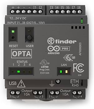
The Arduino™ Opta® is a secure micro Programmable Logic Controller (PLC) with Industrial Internet of Things (IoT) capabilities.
Developed in partnership with Finder®, this device supports both the Arduino programming language and standard IEC-61131-3 PLC programming languages, such as Ladder Diagram (LD), Sequential Function Chart (SFC), Function Block Diagram (FBD), Structured Text (ST), and Instruction List (IL), making it an ideal device for automation engineers.
For Zephyr RTOS, only the M4 is supported for now, making the M7 run the PLC tasks while the M4 core under Zephyr acts as a coprocessor.
Additionally, the device features:
Ethernet compliant with IEEE802.3-2002
16MB QSPI Flash
4 x green color status LEDs
1 x user push-button
1 x reset push-button accessible via pinhole
8 x analog inputs
4 x isolated relay outputs
More information about the board can be found at the ARDUINO-OPTA website. More information about STM32H747XIH6 can be found here:
Supported Features
The current Zephyr arduino_opta_m4 board configuration supports the following hardware features:
Interface |
Controller |
Driver/Component |
|---|---|---|
NVIC |
on-chip |
nested vector interrupt controller |
PINMUX |
on-chip |
pinmux |
GPIO |
on-chip |
gpio |
FLASH |
on-chip |
flash memory |
RNG |
on-chip |
True Random number generator |
IPM |
on-chip |
virtual mailbox based on HSEM |
Other hardware features are not yet supported on Zephyr porting.
The default configuration per core can be found in the defconfig files:
boards/arm/arduino_opta_m4/arduino_opta_m4_defconfig
Pin Mapping
ARDUINO OPTA M4 has access to the 9 GPIO controllers. These controllers are responsible for pin muxing, input/output, pull-up, etc.
For more details please refer to ARDUINO-OPTA website.
Default Zephyr Peripheral Mapping
Status LED1 : PI0
Status LED2 : PI1
Status LED3 : PI3
Status LED4 : PH15
User button : PE4
System Clock
The STM32H747I System Clock can be driven by an internal or external oscillator, as well as by the main PLL clock. By default, the CPU2 (Cortex-M4) System clock is driven at 240MHz. PLL clock is fed by a 25MHz high speed external clock.
Resources sharing
The dual core nature of STM32H747 SoC requires sharing HW resources between the two cores. This is done in 3 ways:
Compilation: Clock configuration is only accessible to M7 core. M4 core only has access to bus clock activation and deactivation.
Static pre-compilation assignment: Peripherals such as a UART are assigned in devicetree before compilation. The user must ensure peripherals are not assigned to both cores at the same time.
Run time protection: Interrupt-controller and GPIO configurations could be accessed by both cores at run time. Accesses are protected by a hardware semaphore to avoid potential concurrent access issues.
Programming and Debugging
Applications for the arduino_opta_m4 use the regular Zephyr build commands.
See Building an Application for more information about application builds.
Flashing
Flashing operation will depend on the target to be flashed and the SoC option bytes configuration. The OPTA has a DFU capable bootloader which can be accessed by connecting the device to the USB, and then pressing the RESET button shortly twice, the RESET-LED on the board will fade indicating the board is in bootloader mode.
By default:
CPU2 (Cortex-M4) boot address is set to 0x08180000 (OB: BOOT_CM4_ADD0)
Zephyr flash configuration has been set to meet these default settings.
Flashing an application to ARDUINO OPTA M4
First, connect the device to your host computer using the USB port to prepare it for flashing. Then build and flash your application.
Here is an example for the Blinky application on M4 core.
# From the root of the zephyr repository
west build -b arduino_opta_m4 samples/basic/blinky
west flash
Starting the application on the ARDUINO OPTA M4
Make sure the option bytes are set to prevent the M4 from auto-starting, and that the M7 side starts the M4 at the correct Flash address.
This can be done by selecting in the Arduino IDE’s “Tools” / “Flash Split” menu the “1.5MB M7 + 0.5MB M4” option, and loading a sketch that contains at least the following code:
#include <RPC.h>

void setup() {
    RPC.begin();
}

void loop() { }
Debugging
Debugging is not yet supported by this board, since the debug port does not have an easy access.