u-blox EVK NINA-B40x
Overview
The u-blox NINA-B4 Evaluation Kit hardware is a Bluetooth low energy module based on the Nordic Semiconductor nRF52833 ARM Cortex-M4F CPU and has support for the following features:
ADC
CLOCK
FLASH
GPIO
I2C
MPU
NVIC
PWM
RADIO (Bluetooth Low Energy)
RTC
Segger RTT (RTT Console)
SPI
UART
USB
WDT
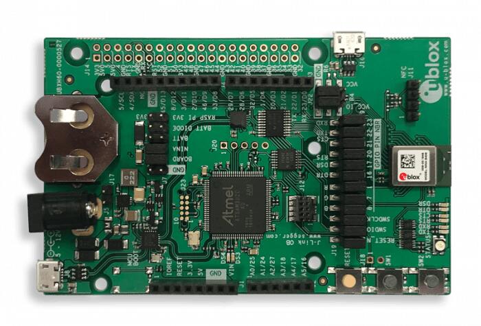
EVK NINA-B4
More information about the NINA-B4 module and the EVK-NINA-B4 can be found at NINA-B40 product page [1] and EVK-NINA-B4 product page [2].
Supported Features
The ubx_evkninab4_nrf52833 board configuration supports the following hardware features:
Interface |
Controller |
Driver/Component |
|---|---|---|
ADC |
on-chip |
adc |
CLOCK |
on-chip |
clock_control |
FLASH |
on-chip |
flash |
GPIO |
on-chip |
gpio |
I2C(M) |
on-chip |
i2c |
MPU |
on-chip |
arch/arm |
NVIC |
on-chip |
arch/arm |
PWM |
on-chip |
pwm |
RADIO |
on-chip |
Bluetooth low energy |
RTC |
on-chip |
system clock |
RTT |
Segger |
console |
SPI(M/S) |
on-chip |
spi |
UART |
on-chip |
serial |
USB |
on-chip |
usb |
WDT |
on-chip |
watchdog |
Other hardware features have not been enabled yet for this board. See EVK-NINA-B4 product page [2] and NINA-B40 Data Sheet [3] for a complete list of EVK NINA-B4 hardware features.
Connections and IOs
LED
LED0 (red) = P0.13
LED1 (green) = P1.01
LED2 (blue) = P1.00
General information on module pin numbering
The numbering of the pins on the module and EVK do not follow the GPIO numbering on the nRF52833 SoC. Please see the NINA-B40 Data Sheet [3] for information on how to map NINA-B40 pins to the pin numbering on the nRF52833 SoC.
The reason for this is the u-blox module family concept where different modules share the same pinout and can be interchanged, see NINA module family Nested design [4].
Programming and Debugging
Applications for the ubx_evkninab4_nrf52833 board configuration can be
built and flashed in the usual way (see Building an Application
and Run an Application for more details); however, the standard
debugging targets are not currently available.
Flashing
Build and flash applications as usual (see Building an Application and Run an Application for more details)
Here is an example for the Hello World application.
Open a terminal program to the USB Serial Port installed when connecting the board and listen for output.
Settings: 115200, 8N1, no flow control.
Then build and flash the application in the usual way.
# From the root of the zephyr repository
west build -b ubx_evknina4_nrf52833 samples/hello_world
west flash
Debugging
Refer to the Nordic nRF5x Segger J-Link page to learn about debugging boards containing a Nordic Semiconductor chip with a Segger IC.
Using UART1
The following approach can be used when an application needs to use more than one UART for connecting peripheral devices:
Add device tree overlay file to the main directory of your application:
&pinctrl {
   uart1_default: uart1_default {
      group1 {
         psels = <NRF_PSEL(UART_TX, 0, 14)>,
                 <NRF_PSEL(UART_RX, 0, 16)>;
      };
   };
   /* required if CONFIG_PM_DEVICE=y */
   uart1_sleep: uart1_sleep {
      group1 {
         psels = <NRF_PSEL(UART_TX, 0, 14)>,
                 <NRF_PSEL(UART_RX, 0, 16)>;
         low-power-enable;
      };
   };
};

&uart1 {
  compatible = "nordic,nrf-uarte";
  current-speed = <115200>;
  status = "okay";
  pinctrl-0 = <&uart1_default>;
  pinctrl-1 = <&uart1_sleep>;
  pinctrl-names = "default", "sleep";
};
In the overlay file above, pin P0.16 is used for RX and P0.14 is used for TX
Use the UART1 as
DEVICE_DT_GET(DT_NODELABEL(uart1))
Overlay file naming
The file has to be named <board>.overlay and placed in the app main directory to be
picked up automatically by the device tree compiler.
Selecting the pins
Pins can be configured in the board pinctrl file. To see the available mappings, open the data sheet for the NINA-B4 at NINA-B40 Data Sheet [3], Section 3 ‘Pin definition’. In the table 7 select the pins marked ‘GPIO_xx’. Note that pins marked as ‘Radio sensitive pin’ can only be used in under-10KHz applications. They are not suitable for 115200 speed of UART.