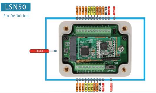
Dragino LSN50 LoRA Sensor Node
Overview
The Dragino LSN50 LoRA Sensor Node for IoT allows users to develop applications with LoraWAN connectivity via the HopeRF / SX1276/SX1278. Dragino LSN50 enables a wide diversity of applications by exploiting low-power communication, ARM® Cortex®-M0 core-based STM32L0 Series features.
This kit provides:
STM32L072CZ MCU
SX1276/SX1278 LoRa Transceiver
Expansion connectors:
PMOD
Li/SOCI2 Unchargable Battery
GPIOs exposed via screw terminals on the carrier board
Housing

More information about the board can be found at the Dragino LSN50 website.
Hardware
The STM32L072CZ SoC provides the following hardware IPs:
Ultra-low-power (down to 0.29 µA Standby mode and 93 uA/MHz run mode)
Core: ARM® 32-bit Cortex®-M0+ CPU, frequency up to 32 MHz
Clock Sources:
1 to 32 MHz crystal oscillator
32 kHz crystal oscillator for RTC (LSE)
Internal 16 MHz factory-trimmed RC ( ±1%)
Internal low-power 37 kHz RC ( ±5%)
Internal multispeed low-power 65 kHz to 4.2 MHz RC
RTC with HW calendar, alarms and calibration
Up to 24 capacitive sensing channels: support touchkey, linear and rotary touch sensors
11x timers:
2x 16-bit with up to 4 channels
2x 16-bit with up to 2 channels
1x 16-bit ultra-low-power timer
1x SysTick
1x RTC
2x 16-bit basic for DAC
2x watchdogs (independent/window)
Up to 84 fast I/Os, most 5 V-tolerant.
Memories
Up to 192 KB Flash, 2 banks read-while-write, proprietary code readout protection
Up to 20 KB of SRAM
External memory interface for static memories supporting SRAM, PSRAM, NOR and NAND memories
Rich analog peripherals (independent supply)
1x 12-bit ADC 1.14 MSPS
2x 12-bit DAC
2x ultra-low-power comparators
11x communication interfaces
USB OTG 2.0 full-speed, LPM and BCD
3x I2C FM+(1 Mbit/s), SMBus/PMBus
4x USARTs (ISO 7816, LIN, IrDA, modem)
6x SPIs (4x SPIs with the Quad SPI)
7-channel DMA controller
True random number generator
CRC calculation unit, 96-bit unique ID
Development support: serial wire debug (SWD), JTAG, Embedded Trace Macrocell™
More information about STM32L072CZ can be found here:
Supported Features
The Zephyr Dragino LSN50 board configuration supports the following hardware features:
Interface |
Controller |
Driver/Component |
|---|---|---|
UART |
on-chip |
serial port-polling; serial port-interrupt |
PINMUX |
on-chip |
pinmux |
GPIO |
on-chip |
gpio |
Other hardware features are not yet supported on this Zephyr port.
The default configuration can be found in the defconfig file:
boards/arm/dragino_lsn50/dragino_lsn50_defconfig
Connections and IOs
Dragino LSN50 Board has GPIO controllers. These controllers are responsible for pin muxing, input/output, pull-up, etc.
Available pins:
For detailed information about available pins please refer to Dragino LSN50 website.
Default Zephyr Peripheral Mapping:
UART_1_TX : PB6
UART_1_RX : PB7
UART_2_TX : PA2
UART_2_RX : PA3
System Clock
Dragino LSN50 System Clock is at 32MHz,
Serial Port
Dragino LSN50 board has 2 U(S)ARTs. The Zephyr console output is assigned to UART1. Default settings are 115200 8N1.
Programming and Debugging
Applications for the dragino_lsn50 board configuration can be built and
flashed in the usual way (see Building an Application and
Run an Application for more details).
Flashing
Dragino LSN50 board requires an external debugger.
Flashing an application to Dragino LSN50
Here is an example for the Hello World application.
Connect the Dragino LSN50 to a STLinkV2 to your host computer using the USB port, then run a serial host program to connect with your board. For example:
$ minicom -D /dev/ttyACM0
Then build and flash the application:
# From the root of the zephyr repository
west build -b dragino_lsn50 samples/hello_world
west flash
You should see the following message on the console:
$ Hello World! arm
Debugging
You can debug an application in the usual way. Here is an example for the Hello World application.
# From the root of the zephyr repository
west build -b dragino_lsn50 samples/hello_world
west debug
