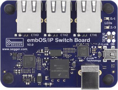
SEGGER IP Switch Board
Overview
The Segger IP Switch Board is a Evaluation board based on NXP Kinetis K66 MCU. It comes with Micrel/Microchip KSZ8794CNX integrated 4-port 10/100 managed Ethernet switch with Gigabit RGMII/MII/RMII interface.
KSZ8794CNX enables evaluation for switch functions
On-board debug probe J-Link-OB for programming

Hardware
MK66FN2M0VMD18 MCU (180 MHz, 2 MB flash memory, 256 KB RAM, low-power, crystal-less USB
Dual role USB interface with micro-B USB connector
2 User LED
On-board debug probe J-Link-OB for programming
Micrel/Microchip Ethernet Switch KSZ8794CNX with 3 RJ45 connectors
For more information about the K66F SoC and IP-K66F board:
Supported Features
The ip_k66f board configuration supports the following hardware features:
Interface |
Controller |
Driver/Component |
|---|---|---|
NVIC |
on-chip |
nested vector interrupt controller |
SYSTICK |
on-chip |
systick |
PINMUX |
on-chip |
pinmux |
GPIO |
on-chip |
gpio |
WATCHDOG |
on-chip |
watchdog |
FLASH |
on-chip |
soc flash |
RTC |
on-chip |
rtc |
The default configuration can be found in the defconfig file:
boards/arm/ip_k66f/ip_k66f_defconfig
Micrel/Microchip KSZ8794CNX Ethernet Switch is not currently supported.
Connections and IOs
The K66F SoC has five pairs of pinmux/gpio controllers.
Name |
Function |
Usage |
|---|---|---|
PTA8 |
GPIO |
Red LED |
PTA10 |
GPIO |
RED LED |
System Clock
The K66F SoC is configured to use the 12 MHz low gain crystal oscillator on the board with the on-chip PLL to generate a 180 MHz system clock.
Serial Port
The K66F SoC has six UARTs. None of them are used.
Programming and Debugging
Build and flash applications as usual (see Building an Application and Run an Application for more details).
Configuring a Debug Probe
A debug probe is used for both flashing and debugging the board. This board is configured by default to use the OpenSDA J-Link Onboard Debug Probe.
OpenSDA J-Link Onboard Debug Probe
Install the Enabling BOSSAC on Windows Native [Experimental] and make sure they are in your search path.
Follow the instructions in OpenSDA J-Link Onboard Debug Probe to program the OpenSDA J-Link Generic Firmware for V3.2 Bootloader. Note that Segger does provide an OpenSDA J-Link Board-Specific Firmware for this board, however it is not compatible with the DAPLink bootloader.
The default flasher is jlink using the built-in SEGGER Jlink interface.
Flashing
Here is an example for the Blinky application.
# From the root of the zephyr repository
west build -b ip_k66f samples/basic/blinky
west flash
Red LED0 should blink at 1 second delay.
Debugging
Here is an example for the Blinky application.
# From the root of the zephyr repository
west build -b ip_k66f samples/basic/blinky
west debug
Step through the application in your debugger.
Serial console
The ip_k66f board only uses Segger’s RTT console for providing serial
console. There is no physical serial port available.
To communicate with this board one needs in one console:
/opt/SEGGER/JLink_V664/JLinkRTTLogger -Device MK66FN2M0XXX18 -RTTChannel 1 -if SWD -Speed 4000 ~/rtt.log
In another one:
nc localhost 19021
