Evaluation Board Setup (PCA10001/PCA10003)
The following instructions describe how to set up the Evaluation Board:
- Connect the Evaluation Board to the PC.
If you are using SoftDevice S110 (Bluetooth):
- Program the S110 SoftDevice (see the nRF51822 EK User Guide).
- Connect the Master Emulator (nRF2739) to the PC.
For all examples the same hardware setup is used.
Some of the GPIO pins are already defined to have a special purpose:
- PIN 8 - is used for UART RTS
- PIN 9 - is used for UART TX
- PIN 10 - is used for UART CTS
- PIN 11 - is used for UART RX
- PIN 16 - is used for BUTTON0
- PIN 17 - is used for BUTTON1
- PIN 18 - is used for LED0
- PIN 19 - is used for LED1
Configure your terminal application for 38400 bauds, 8 data bits, 1 stop bit and Flow Control RTS/CTS enabled.
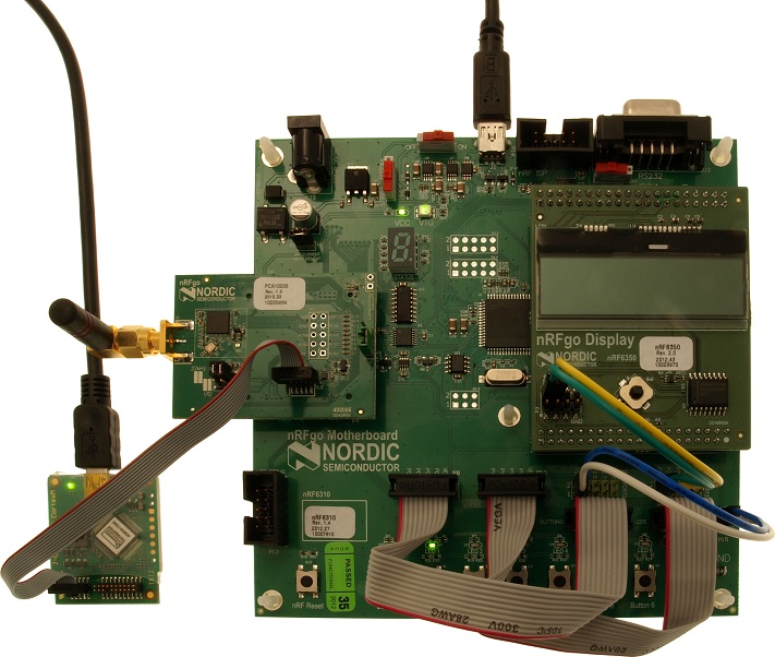
nRFgo Motherboard Setup (nRF6310)
The following instructions describe how to set up the nRFgo Motherboard (the names in bold refer to the silk print on the Motherboard):
- Mount nRFgo carrier board and the PCA10004/PCA10005 module.
- Connect a 10p flat cable (2.54 mm, included in nRFgo Starter Kit) from PORT0 to the BUTTONS connector. In doing so, ensure that P0.0 is connected to BUTTON 1.
- Connect another 10p flat cable (2.54 mm, also included in nRFgo Starter Kit) from PORT1 to the LEDS connector. In doing so, ensure that P1.0 is connected to LED 1. (Refer to the image in 'Connect the hardware' section of the 'Getting Started Guide' to see this connection)
- Connect a 2p cable from RX-TX to P2.0 and P2.1, so that RX is connected to P2.0 and TX is connected to P2.1.
- Connect a 2p cable from P3.0-P3.1 to SDA-SCL, so that P3.0 is connected to SCL and P3.1 is connected to SDA in the display extension board.
- Connect the nRFgo Motherboard (nRF6310) to the PC using a USB cable.
If you are using SoftDevice S110 (Bluetooth):
- Program the S110 SoftDevice (see the nRF51822 DK User Guide).
- Connect the Master Emulator (nRF2739) to the PC.
nRFgo Motherboard Setup
For all examples the same hardware setup is used.
Some of the GPIO pins are already defined to have a special purpose:
- PIN 0 to 7 - is used for buttons (Named P0.0-P0.7 on the nRF6310 Motherboard).
- PIN 8 to 15 - is used for LEDs (Named P1.0-P1.7 on the nRF6310 Motherboard).
- PIN 16 - is used for serial RX (P2.0 on the nRF6310 Motherboard).
- PIN 17 - is used for serial TX (P2.1 on the nRF6310 Motherboard).
- PIN 24 - is used for display clock - SCL (P3.0 on the nRF6310 Motherboard).
- PIN 25 - is used for display data - SDA (P3.1 on the nRF6310 Motherboard).
Configure your terminal application for 38400 bauds, 8 data bits and 1 stop bit. The nRF6310 examples do not use any flow control.
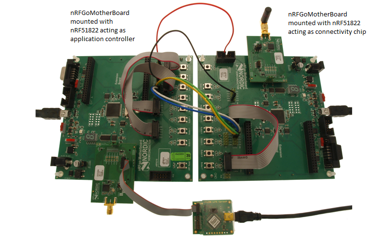
nRFgo Motherboard Setup - Serialization
Terminology
This section uses the following terminology.
Application Board - The nRFgo MotherBoard mounted with nRF51822 acting as application controller.
Connectivity Board - The nRFgo MotherBoard mounted with nRF51822 acting as connectivity chip.
nRFgo Motherboard Setup (nRF6310)
The following instructions describe how to set up two nRFgo Motherboards to be used for testing a serialized Bluetooth Application.
The Application Board will have the nRF51822 that will act as an application controller mounted on it. In this chip, an example application that has been modified to use the rpc_command_encoder, rpc_evt_decoder, and rpc_transport, instead of the nrf518_lib_ble_s110, will be running.
The Connectivity Board will have the nRF51822 that will act as a connectivity chip mounted on it. This will run the application that will decode the serialized commands received from the application controller and execute the corresponding S110 SoftDevice API. This will be done using the rpc_cmd_decoder. The connectivity chip will then encode return value of S110 SoftDevice API and transmit it back as the response to the application controller.
The connectivity chip will also encode all events from the S110 SoftDevice using the rpc_event_encoder and transmit them to the application controller.
- Mount two nRFgo Motherboards (nRF6310) with a PCA10004/PCA10005 module on each.
Application Board setup
- Connect a 10p flat cable (2.54 mm, included in nRFgo Starter Kit) from PORT0 to the BUTTONS connector. In doing so, ensure that P0.0 is connected to BUTTON 1.
- Connect another 10p flat cable (2.54 mm, also included in nRFgo Starter Kit) from PORT1 to the LEDS connector. In doing so, ensure that P1.0 is connected to LED 1. (Refer to the image in 'Connect the hardware' section of the 'Getting Started Guide' to see this connection)
Connectivity Board setup
- Connect a 10p flat cable (2.54 mm, included in nRFgo Starter Kit) from PORT1 to the LEDS connector. In doing so, ensure that P1.0 is connected to LED 1. (Refer to the image in 'Connect the hardware' section of the 'Getting Started Guide' to see this connection)
- Connect both the Motherboards to the PC using USB cables.
nRFgo Motherboard Setup for Serialization examples.
Inter-board connections.
- RX-TX: Connect P2.0 (RX) on Application Board to P2.1 (TX) on Connectivity Board.
- TX-RX: Connect P2.1 (TX) on Application Board to P2.0 (RX) on Connectivity Board.
- CTS-RTS: Connect P2.2 (CTS) on Application Board to P2.3 (RTS) on Connectivity Board.
- RTS-CTS: Connect P2.3 (RTS) on Application Board to P2.2 (CTS) on Connectivity Board.
- Reset line: Connect P3.6 on Application Board to Reset pin nRF Debug P12.7 on Connectivity Board.
- Ground: Connect GND pin (choose any available GND pin) on Application Board to a GND pin on Connectivity Board.
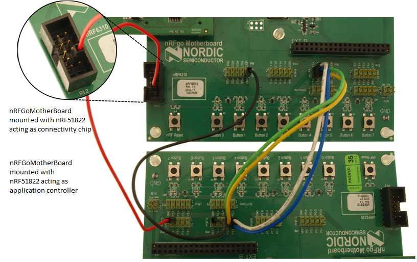
Close-up picture of nRFgo Motherboard inter-board connections.
- Note
- For all serialization examples, this same hardware setup is used.
Prepare nRF51822 boards
- Connect the Master Emulator (nRF2739) to the PC.
- Note
nrfjprog is expected to be located in the windows system path, PATH%, for the above command to work, otherwise full path to nrfjprog must be given.
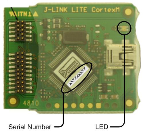
J-Link Lite CortexM-9 SNR location (Serial number).
Flashing of nRF51822 Connectivity Chip software
- Detach the reset cable from pin P12.7 on the Connectivity Board.
- Attach the J-Link Lite CortexM-9 to the Connectivity Board.
- Open the ble_sdk_app_connectivity project in Keil, compile, and flash.
- Detach the J-Link Lite CortexM-9 from the Connectivity Board.
- Attach the reset cable to pin P12.7 on the Connectivity Board.
Flashing of Serialized <i>Bluetooth</i> Application
- Attach the J-Link Lite CortexM-9 to the Application board.
- Open a serialized Bluetooth Application project in Keil, compile, and flash the application to the Application board, e.g. ble_sdk_app_hrs_ser.
Verifying the application
Use the following steps to verify that the application is able to connect to the nRF51822 connectivity chip and start advertising.
- Power on the Connectivity Board.
- Power on the Application board.
- On the Application board.
- Verify LED 0 is lit, indicating that the serialized Bluetooth Application has successfully transmitted serialized commands to the Connectivity Chip and that the latter has started advertising.
GPIO Pin assignments
Some of the GPIO pins are already defined to have a special purpose:
- PIN 0 to 7 - is used for buttons (Named P0.0-P0.7 on the nRF6310 Motherboard).
- PIN 8 to 15 - is used for LEDs (Named P1.0-P1.7 on the nRF6310 Motherboard).
- PIN 16 - is used for serial RX (P2.0 on the nRF6310 Motherboard).
- PIN 17 - is used for serial TX (P2.1 on the nRF6310 Motherboard).
- PIN 18 - is used as Clear To Send pin for Hardware Flow Control (P2.2 on the nRF6310 Motherboard).
- PIN 19 - is used as Ready To Send pin for Hardware Flow Control (P2.3 on the nRF6310 Motherboard).
- PIN 30 - is used for reset signal from Application board to the connectivity chip.

 1.8.3.1
