Evaluation Board Setup (PCA10001/PCA10003)
Terminology
Application Board - The Evaluation Board with nRF51822 acting as application controller.
Connectivity Board - The Evaluation Board with nRF51822 acting as connectivity chip.
This section uses the following terminology.
Evaluation Board Setup (PCA10001)
The following instructions describe how to set up two Evaluation Board to be used for testing a serialized Bluetooth Application.
The Application Board has the nRF51822 that acts as an application controller mounted on it. In this chip, an example application that has been modified to use the stubbed SoftDevice sends serialized S110 SoftDevice API commands via UART or SPI.
The Connectivity Board has the nRF51822 that acts as a connectivity chip mounted on it. This chip runs application that receives and decodes serialized commands and then execute the corresponding S110 SoftDevice API. The connectivity chip also encodes return values and events from S110 SoftDevice API and transmits it to the application controller.
Inter-board connections (PCA10001)
- Note
- Evaluation Board PCA10001 does not have RESET pin on the PCB, connectivity chip must be resetted manually or by the debugger.
-
If reset button does not work please disconnect and connect USB cable to Evaluation Board.
SPI inter-board connections:
- MISO - MISO: Connect P0.22 (MISO) on Application Board to P0.20 (MISO) on Connectivity Board.
- MOSI - MOSI: Connect P0.20 (MOSI) on Application Board to P0.22 (MOSI) on Connectivity Board.
- SCK - SCK: Connect P0.23 (SCK) on Application Board to P0.23 (SCK) on Connectivity Board.
- CS - CS: Connect P0.21 (CS) on Application Board to P0.21 (CS) on Connectivity Board.
- nREQ: Connect P0.24 (nREQ) on Application Board to P0.24 (nREQ) on Connectivity Board.
- nRDY: Connect P0.25 (nRDY) on Application Board to P0.25 (nRDY) on Connectivity Board. (Only SPI 6-wire configuration)
- Ground: Connect GND pin (choose any available GND pin) on Application Board to a GND pin on Connectivity Board.
UART inter-board connections:
- RX - TX: Connect P0.20 (RX) on Application Board to P0.22 (TX) on Connectivity Board.
- TX - RX: Connect P0.22 (TX) on Application Board to P0.20 (RX) on Connectivity Board.
- CTS - RTS: Connect P0.23 (CTS) on Application Board to P0.23 (RTS) on Connectivity Board.
- RTS - CTS: Connect P0.21 (RTS) on Application Board to P0.21 (CTS) on Connectivity Board.
- Ground: Connect GND pin (choose any available GND pin) on Application Board to a GND pin on Connectivity Board.
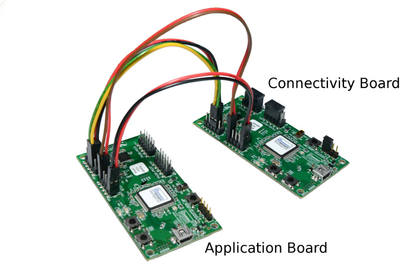
Evaluation Boards UART and SPI Setup for Serialization examples.
- Note
- Boards in the picture have connected VCC so only Application Board should be connected via USB cable.
Prepare Evaluation Boards
- Note
nrfjprog is expected to be located in the windows system path, PATH%, for the above command to work, otherwise full path to nrfjprog must be given.
Flashing of nRF51822 Connectivity Chip firmware
- Attach the USB cable to the Connectivity Board.
- Open the BLE S110 Connectivity Chip project in Keil, compile, and flash.
- Reset Connectivity Board using Debugger.
Flashing of Serialized Bluetooth Application
- Attach the USB Cable to the Application board.
- Open a serialized Bluetooth Application project in Keil, compile, and flash the application to the Application board.
Serialized projects are in project directories with the name ended 'serialization'. The path to projects:
- Board PCA10001: <InstallFolder>\Nordic\nrf51822\Board\pca10001\s110
Verifying the application
Use the following steps to verify that the application is able to connect to the nRF51822 connectivity chip and start advertising.
- Power on the Connectivity Board.
- Power on the Application board.
- On the Application board:
- Verify LED 0 is lit, indicating that the serialized Bluetooth Application has successfully started.
nRFgo Motherboard Setup (nRF6310)
Terminology
This section uses the following terminology.
Application Board - The nRFgo MotherBoard mounted with nRF51822 acting as application controller.
Connectivity Board - The nRFgo MotherBoard mounted with nRF51822 acting as connectivity chip.
nRFgo Motherboard Setup (nRF6310)
The following instructions describe how to set up two nRFgo Motherboards to be used for testing a serialized Bluetooth Application.
The Application Board has the nRF51822 that acts as an application controller mounted on it. In this chip, an example application that has been modified to use the stubbed SoftDevice sends serialized S110 SoftDevice API commands via UART or SPI.
The Connectivity Board has the nRF51822 that acts as a connectivity chip mounted on it. This chip runs application that receives and decodes serialized commands and then execute the corresponding S110 SoftDevice API. The connectivity chip also encodes return values and events from S110 SoftDevice API and transmits it to the application controller.
- Mount two nRFgo Motherboards (nRF6310) with a PCA10004/PCA10005 module on each.
Application Board setup
- Connect a 10p flat cable (2.54 mm, included in nRFgo Starter Kit) from PORT0 to the BUTTONS connector. In doing so, ensure that P0.0 is connected to BUTTON 1.
- Connect another 10p flat cable (2.54 mm, also included in nRFgo Starter Kit) from PORT1 to the LEDS connector. In doing so, ensure that P1.0 is connected to LED 1. (Refer to the image in 'Connect the hardware' section of the 'Getting Started Guide' to see this connection)
Connectivity Board setup
- Connect a 10p flat cable (2.54 mm, included in nRFgo Starter Kit) from PORT1 to the LEDS connector. In doing so, ensure that P1.0 is connected to LED 1. (Refer to the image in 'Connect the hardware' section of the 'Getting Started Guide' to see this connection)
- Connect both the Motherboards to the PC using USB cables.
Inter-board connections (nRF6310)
SPI inter-board connections:
- MISO - MISO: Connect P2.6 (MISO) on Application Board to P2.4 (MISO) on Connectivity Board.
- MOSI - MOSI: Connect P2.4 (MOSI) on Application Board to P2.6 (MOSI) on Connectivity Board.
- SCK - SCK: Connect P2.5 (SCK) on Application Board to P2.5 (SCK) on Connectivity Board.
- CS - CS: Connect P2.7 (CS) on Application Board to P2.7 (CS) on Connectivity Board.
- nREQ: Connect P3.4 (nREQ) on Application Board to P3.4 (nREQ) on Connectivity Board.
- nRDY: Connect P3.5 (nRDY) on Application Board to P3.5 (nRDY) on Connectivity Board. (Only SPI 6-wire configuration)
- RST: Connect P3.6 on Application Board to Reset pin nRF Debug P12.7 on Connectivity Board.
- Ground: Connect GND pin (choose any available GND pin) on Application Board to a GND pin on Connectivity Board.
UART inter-board connections:
- RX - TX: Connect P2.0 (RX) on Application Board to P2.1 (TX) on Connectivity Board.
- TX - RX: Connect P2.1 (TX) on Application Board to P2.0 (RX) on Connectivity Board.
- CTS - RTS: Connect P2.2 (CTS) on Application Board to P2.3 (RTS) on Connectivity Board.
- RTS - CTS: Connect P2.3 (RTS) on Application Board to P2.2 (CTS) on Connectivity Board.
- RST: Connect P3.6 on Application Board to Reset pin nRF Debug P12.7 on Connectivity Board.
- Ground: Connect GND pin (choose any available GND pin) on Application Board to a GND pin on Connectivity Board.
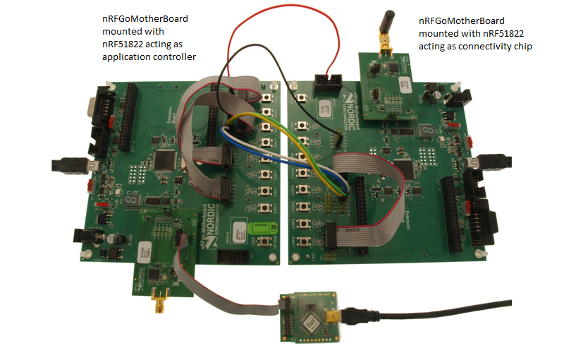
nRFgo Motherboard UART Setup for Serialization examples.
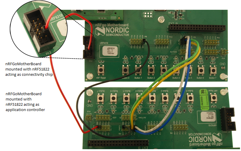
Close-up picture of nRFgo Motherboard UART inter-board connections.
- Note
- For all serialization examples, this same hardware setup is used.
Prepare nRF51822 boards
- Connect the Master Emulator (nRF2739) to the PC.
- Note
nrfjprog is expected to be located in the windows system path, PATH%, for the above command to work, otherwise full path to nrfjprog must be given.
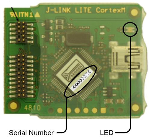
J-Link Lite CortexM-9 SNR location (Serial number).
Flashing of nRF51822 Connectivity Chip firmware
- Detach the reset cable from pin P12.7 on the Connectivity Board.
- Attach the J-Link Lite CortexM-9 to the Connectivity Board.
- Open the ble_connectivity_app_path_sub_sec project in Keil, compile, and flash.
- Detach the J-Link Lite CortexM-9 from the Connectivity Board.
- Attach the reset cable to pin P12.7 on the Connectivity Board.
Flashing of Serialized Bluetooth Application
- Attach the J-Link Lite CortexM-9 to the Application board.
- Open a serialized Bluetooth Application project in Keil, compile, and flash the application to the Application board.
Serialized projects are in project directories with the name ended 'serialization'. The path to projects:
- Board nRF6310: <InstallFolder>\Nordic\nrf51822\Board\nrf6310\s110
Verifying the application
Use the following steps to verify that the application is able to connect to the nRF51822 connectivity chip and start advertising.
- Power on the Connectivity Board.
- Power on the Application board.
- On the Application board.
- Verify LED 0 is lit, indicating that the serialized Bluetooth Application has successfully transmitted serialized commands to the Connectivity Chip and that the latter has started advertising.
GPIO Pin assignments
Some of the GPIO pins are already defined to have a special purpose:
- PIN 0 to 7 - is used for buttons (Named P0.0 - P0.7 on the nRF6310 Motherboard).
- PIN 8 to 15 - is used for LEDs (Named P1.0 - P1.7 on the nRF6310 Motherboard).
- PIN 30 - is used for reset signal from Application board to the connectivity chip.
UART - Application Board and Connectivity Board pins assignment:
- PIN 16 - is used for serial RX (P2.0 on the nRF6310 Motherboard).
- PIN 17 - is used for serial TX (P2.1 on the nRF6310 Motherboard).
- PIN 18 - is used as Clear To Send pin for Hardware Flow Control (P2.2 on the nRF6310 Motherboard).
- PIN 19 - is used as Ready To Send pin for Hardware Flow Control (P2.3 on the nRF6310 Motherboard).
SPI Master - Application Board pins assignment:
- PIN 23 - is used for Serial Clock - SCK (P2.7 on the nRF6310 Motherboard).
- PIN 20 - is used for Master Output Slave Input - MOSI (P2.4 on the nRF6310 Motherboard).
- PIN 22 - is used for Master Input Slave Output - MISO (P2.6 on the nRF6310 Motherboard).
- PIN 21 - is used for Cabel Select - CS (P2.5 on the nRF6310 Motherboard).
- PIN 28 - is used for Request line - nREQ (P3.4 on the nRF6310 Motherboard).
- PIN 29 - is used for Ready line - nRDY (P3.5 on the nRF6310 Motherboard).
[only 6-wire]
SPI Slave - Connectivity Board pins assignment:
- PIN 23 - is used for Serial Clock - SCK (P2.7 on the nRF6310 Motherboard).
- PIN 20 - is used for Master Input Slave Output - MISO (P2.4 on the nRF6310 Motherboard).
- PIN 22 - is used for Master Output Slave Input - MOSI (P2.6 on the nRF6310 Motherboard).
- PIN 21 - is used for Cabel Select - CS (P2.5 on the nRF6310 Motherboard).
- PIN 28 - is used for Request line - nREQ (P3.4 on the nRF6310 Motherboard).
- PIN 29 - is used for Ready line - nRDY (P3.5 on the nRF6310 Motherboard).
[only 6-wire]

 1.8.3.1
