u-blox EVK-BMD-30/35: BMD-300-EVAL, BMD-301-EVAL, and BMD-350-EVAL
Overview
The BMD-300-EVAL, BMD-301-EVAL, and BMD-350-EVAL hardware provides support for the u-blox BMD-300, BMD-301, and BMD-350 Bluetooth 5 modules, based on the Nordic Semiconductor nRF52832 ARM Cortex-M4F CPU and the following devices:
ADC
CLOCK
FLASH
GPIO
I2C
MPU
NVIC
PWM
RADIO (Bluetooth Low Energy)
RTC
Segger RTT (RTT Console)
SPI
UART
WDT
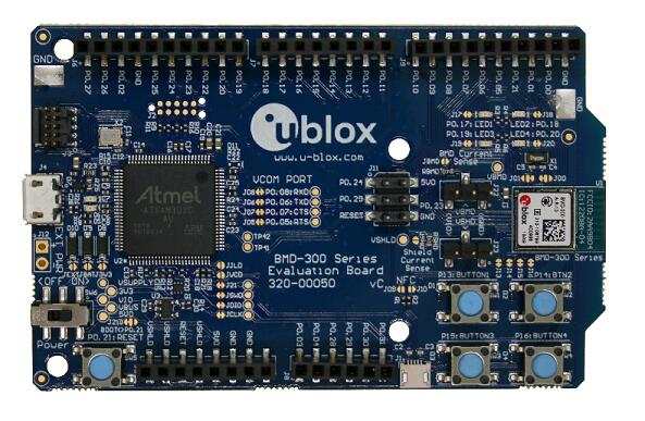
BMD-300-EVAL (Credit: u-blox AG)
Note
The BMD-300-EVAL, BMD-301-EVAL, and BMD-350-EVAL share the same pin headers and assignments. The boards are different only in the module used on the board. The BMD-300 and BMD-301 modules share the same footprint and differ only in the antenna. The BMD-350 module utilizes the nRF52832 CIAA WLCSP package.
More information about the BMD-300-EVAL, BMD-301-EVAL, and BMD-350-EVAL and the respective modules can be found at the u-blox website [1]. All of the Nordic Semiconductor examples for the nRF52 DK (nrf52dk_nrf52832) may be used without modification.
Hardware
The BMD-300/301/350 module on the board contains an internal high-frequency oscillator at 32MHz. There is also a low frequency (slow) oscillator of 32.768kHz. The module itself does not include the slow crystal; however, the EVAL boards do.
Note
When targeting a custom design without a slow crystal, be sure to modify code to utilize the internal RC oscillator for the slow clock.
Supported Features
The BMD-300/301/350-EVAL configuration supports the following hardware features:
Interface |
Controller |
Driver/Component |
|---|---|---|
ADC |
on-chip |
adc |
CLOCK |
on-chip |
clock_control |
FLASH |
on-chip |
flash |
GPIO |
on-chip |
gpio |
I2C(M) |
on-chip |
i2c |
MPU |
on-chip |
arch/arm |
NVIC |
on-chip |
arch/arm |
PWM |
on-chip |
pwm |
RADIO |
on-chip |
Bluetooth |
RTC |
on-chip |
system clock |
RTT |
Segger |
console |
SPI(M/S) |
on-chip |
spi |
UART |
on-chip |
serial |
WDT |
on-chip |
watchdog |
Other hardware features have not been enabled yet for this board. See the u-blox website [1] for a complete list of BMD-300/301/350-EVAL hardware features.
Connections and IOs
LED
LED1 (red) = P0.17
LED2 (red) = P0.18
LED3 (green) = P0.19
LED4 (green) = P0.20
D5 (red) = OB LED 1
D6 (green) = OB LED 2
External Connectors
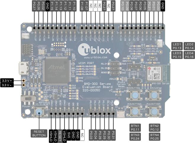
BMD-300-EVAL pin-out (Credit: u-blox AG)
Note
The BMD-300-EVAL, BMD-301-EVAL, and BMD-350-EVAL share the same pin headers and assignments. The BMD-300-EVAL is shown here.
Note
The pin numbers noted below are referenced to the pin 1 markings on the BMD-300/301/350-EVAL for each header
J-Link Prog Connector (J2)
PIN # |
Signal Name |
|---|---|
1 |
VDD |
2 |
IMCU_TMSS |
3 |
GND |
4 |
IMCU_TCKS |
5 |
V5V |
6 |
IMCU_TDOS |
7 |
Cut off |
8 |
IMCU_TDIS |
9 |
Cut off |
10 |
IMCU_RESET |
Debug OUT (J3)
PIN # |
Signal Name |
|---|---|
1 |
EXT_VTG |
2 |
EXT_SWDIO |
3 |
GND |
4 |
EXT_SWDCLK |
5 |
GND |
6 |
EXT_SWO |
7 |
N/C |
8 |
N/C |
9 |
EXT_GND_DETECT |
10 |
EXT_RESET |
Auxiliary (J9)
PIN # |
Signal Name |
|---|---|
1 |
P0.10 |
2 |
P0.09 |
3 |
P0.08 |
4 |
P0.07 |
5 |
P0.06 |
6 |
P0.05 / AIN3 |
7 |
P0.21 / RESET |
8 |
P0.01 / XL2 |
9 |
P0.00 / XL1 |
10 |
GND |
Arduino Headers
Power (J5)
PIN # |
Signal Name |
BMD-300/301/350 Functions |
|---|---|---|
1 |
VSHLD |
N/A |
2 |
VSHLD |
N/A |
3 |
RESET |
P0.21 / RESET |
4 |
VSHLD |
N/A |
5 |
V5V |
N/A |
6 |
GND |
N/A |
7 |
GND |
N/A |
8 |
N/C |
N/A |
Analog in (J8)
PIN # |
Signal Name |
BMD-300/301/350 Functions |
|---|---|---|
1 |
A0 |
P0.03 / AIN1 |
2 |
A1 |
P0.04 / AIN2 |
3 |
A2 |
P0.28 / AIN4 |
4 |
A3 |
P0.29 / AIN5 |
5 |
A4 |
P0.30 / AIN6 |
6 |
A5 |
P0.31 / AIN7 |
Digital I/O (J7)
PIN # |
Signal Name |
BMD-300/301/350 Functions |
|---|---|---|
1 |
D7 |
P0.18/TRACEDATA[0]/SWO |
2 |
D6 |
P0.17 |
3 |
D5 |
P0.16/TRACEDATA[1] |
4 |
D4 |
P0.15/TRACEDATA[2] |
5 |
D3 |
P0.14/TRACEDATA[3] |
6 |
D2 |
P0.13 |
7 |
D1 (TX) |
P0.12 |
8 |
D0 (RX) |
P0.11 |
Digital I/O (J6)
PIN # |
Signal Name |
BMD-300/301/350 Functions |
|---|---|---|
1 |
SCL |
P0.27 |
2 |
SDA |
P0.26 |
3 |
AREF |
P0.02/AIN0 |
4 |
GND |
N/A |
5 |
D13 (SCK) |
P0.25 |
6 |
D12 (MISO) |
P0.24 |
7 |
D11 (MOSI) |
P0.23 |
8 |
D10 (SS) |
P0.22 |
9 |
D9 |
P0.20/TRACECLK |
10 |
D8 |
P0.19 |
J11
PIN # |
Signal Name |
BMD-300/301/350 Functions |
|---|---|---|
1 |
D12 (MISO) |
P0.24 |
2 |
V5V |
N/A |
3 |
D13 (SCK) |
P0.25 |
4 |
D11 (MOSI) |
P0.23 |
5 |
RESET |
N/A |
6 |
N/A |
N/A |
Programming and Debugging
Flashing
Follow the instructions in the Nordic nRF5x Segger J-Link page to install and configure all the necessary software. Further information can be found in Flashing. Then build and flash applications as usual (see Building an Application and Run an Application for more details).
Here is an example for the Hello World application.
First, run your favorite terminal program to listen for output.
$ minicom -D <tty_device> -b 115200
Replace <tty_device> with the port where the
BMD-300/301/350-EVAL can be found. For example, under Linux,
/dev/ttyACM0.
Then build and flash the application in the usual way.
# From the root of the zephyr repository
west build -b ubx_bmd300eval_nrf52832 samples/hello_world
west flash
Debugging
Refer to the Nordic nRF5x Segger J-Link page to learn about debugging u-blox boards with a Segger J-LINK-OB IC.