Electronut Labs Blip
Overview
The Electronut Labs Blip hardware provides support for the Nordic Semiconductor nRF52840 ARM Cortex-M4F CPU and the following devices:
ADC
CLOCK
FLASH
GPIO
I2C
MPU
NVIC
PWM
RADIO (Bluetooth Low Energy and 802.15.4)
RTC
Segger RTT (RTT Console)
SPI
UART
USB
WDT
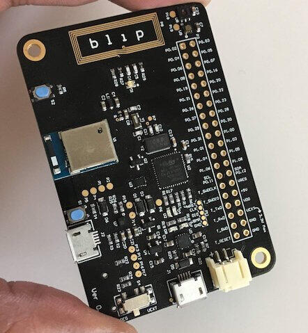
Electronut Labs Blip (Credit: Electronut Labs)
More information about the board is available at https://github.com/electronut/ElectronutLabs-blip.
Hardware
Blip has two external oscillators. The frequency of the slow clock is 32.768 kHz. The frequency of the main clock is 32 MHz.
Supported Features
The nrf52840_blip board configuration supports the following hardware features currently:
Interface |
Controller |
Driver/Component |
|---|---|---|
ADC |
on-chip |
adc |
CLOCK |
on-chip |
clock_control |
FLASH |
on-chip |
flash |
GPIO |
on-chip |
gpio |
I2C(M) |
on-chip |
i2c |
MPU |
on-chip |
arch/arm |
NVIC |
on-chip |
arch/arm |
PWM |
on-chip |
pwm |
RADIO |
on-chip |
Bluetooth, ieee802154 |
RTC |
on-chip |
system clock |
RTT |
Segger |
console |
SPI(M/S) |
on-chip |
spi |
UART |
on-chip |
serial |
USB |
on-chip |
usb |
WDT |
on-chip |
watchdog |
Connections and IOs
LED
LED1 (green) = P0.13
LED2 (red) = P0.14
LED3 (blue) = P0.15
UART
BMP does not support hardware flow control, so only RX/TX pins are connected.
TX = P0.6
RX = P0.8
I2C
I2C pins connected to onboard sensors:
SDA = P0.12
SCL = P0.11
SPI
SCK = P0.25
MOSI = P1.02
MISO = P0.24
MicroSD is connected to these pins, and CS pin is connected to P0.17.
Programming and Debugging
Applications for the nrf52840_blip board configuration can be
built and flashed in the usual way (see Building an Application
and Run an Application for more details); The onboard Black Magic
Probe debugger presents itself as two USB-serial ports. On Linux,
they may come up as /dev/ttyACM0 and /dev/ttyACM1. The first
one of these (/dev/ttyACM0 here) is the debugger port.
GDB can directly connect to this port without requiring a GDB server by specifying
target external /dev/ttyACM0. The second port acts as a
serial port, connected to the SoC.
Flashing
Applications are flashed and run as usual (see Building an Application and Run an Application for more details).
Here is an example for the Hello World application.
First, run your favorite terminal program to listen for output.
$ minicom -D <tty_device> -b 115200
Replace <tty_device> with the serial port of Black Magic Probe.
For example, under Linux, /dev/ttyACM1.
Then build and flash the application in the usual way.
# From the root of the zephyr repository
west build -b nrf52840_blip samples/hello_world
west flash
Debugging
Debug and attach configurations are available using Black Magic Probe, and
ninja debug, or ninja attach (or with make) are available.
NOTE: You may need to press the reset button once after using ninja flash
to start executing the code. (not required with debug or attach)